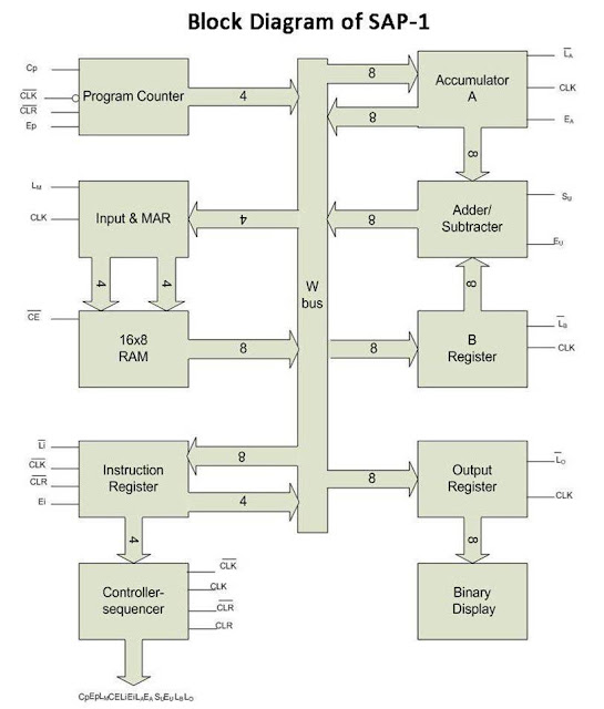
SAP-1 Architecture
The Simple-As-Possible (SAP)-1 computer is a
very basic
model of a microprocessor explained
by Albert Paul Malvino. The SAP-1 design
contains the basic necessities for a functional
Microprocessor. Its primary
purpose is to develop
a basic understanding of how a microprocessor
works,
interacts with memory and other parts of
the system like input and output. The
instruction
set is very limited and is simple.
SAP (Simple-As-Possible)-1 is the first stage in the
evolution toward modern computers.
•SAP is Simple-As-Possible Computer. The type of
computer
is specially designed for the academic
purpose and nothing has to do with the
commercial use. The architecture is 8 bits and
comprises of 16 X 8 memory i.e.
16 memory
location with 8 bits in each location, therefore
, need 4 address
lines which either comes from
the PC (Program Counter which may be called
instruction pointer) during computer run phase or
may come from the 4 address
switches during
the program phase. All instructions (5 only) get
stored in this
memory. It means SAP cannot store
program having more than 16 instructions.
•SAP can only perform addition and subtraction
and no
logical operation. These arithmetic
operations are performed by an adder/subtractor
unit.
•There is one general purpose register (B register)
used
to hold one operand of the arithmetic
operation while another is kept by the
accumulator register of the SAP-1.
•In addition, there are 8 LEDs which work as
output unit
and connected with the 8 bit output
register.
•All timely moment of data or activities are performed by
the controller/sequencer part of the SAP-1.
•Program Counter
• It
counts from 0000 to 1111.
• It
signals the memory address of next instruction to be fetched
and executed.
•Inputs and MAR (Memory Address
Register)
During
a computer run, the address in PC is latched into Memory
Address Register
(MAR).
•The RAM
• The
program code to be executed and data for SAP1 computer is
stored here.
• During
a computer run, the RAM receives 4-bit addresses from
MAR and a read operation
is performed. Hence, the instruction or
data word stored in RAM is placed on
the W bus for use by some
other part of the computer.
• It
is asynchronous RAM, which means that the output data is
available as soon as
valid address and control signal are applied.
•Instruction Register
• IR
contains the instruction (composed of OPCODE+ADDRESS) to
be executed by SAP1
computer.
•Controller-Sequencer
• It
generates the control signals for each block so that actions
occur in desired
sequence. CLK signal is used to synchronize the
overall operation of the SAP1
computer.
• A
12-bit word comes out of the Controller-Sequencer block. This
control word
determines how the registers will react to the next
positive CLK edge.
•Accumulator
• It is a 8-bit buffer register that stores intermediate
results
during a computer run.
• It is always one of the operands of ADD, SUB and OUT
instructions.
•Adder/Subtractor
• It
is a 2's complement adder-subtractor.
• This
module is asynchronous (unclocked), which means
that
its contents can change as soon as the input words
change.
•B-register
• It
is 8-bit buffer register which is primarily used to hold the
other operand (one
operand is always accumulator) of
mathematical operations.
•Output Register
• This
registers hold the output of OUT instruction.
•Binary Display
• It
is a row of eight LEDs to show the contents of output
register.
• Binary
display unit is the output device for the SAP-1
microprocessor.

Comments
Post a Comment